Catania Astrophysical Observatory Laboratory for Detectors
")
")
A new type of position sensor (Complementary Metal Oxide Semiconductor Active Pixel Sensor or CMOS-APS) used as readout system in MCP-based intensified photon counters, has been used at our laboratory few years ago with good success.
The CMOS technology, allows to integrate "on chip" the pixel addressing and the readout circuits as well as the analogue-to-digital converters. The highly parallel structure of the APS allows a count rate dynamic range larger than that obtainable with photon counting systems based on intensified CCD. Other two important characteristics, fundamental in space applications, have to be added: CMOS devices use a single 3.3 V power supply and show a better radiation hardness than CCDs.
The CCD technology, developed more than twenty years ago and improved during these years, is well known and is appreciated in many fields for the high quantum efficiency and the low readout noise even at relatively high scan rates. The novel CMOS-APS technology is in continuous evolution, and, at the moment, a slightly higher readout noise characterizes this technology. But this parameter, in photon counting systems can be overcome by setting a higher MCP gain. The other difference, in favor of CCD, is the fill factor that while for the CCD is 100 %, for the CMOS-APS is not higher than 60 %. However this parameter is not very critical for the performance of intensified systems. The developed system is basically constituted by a Micro Channel Plate (MCP) with a phosphor screen coupled to a CMOS-APS through a relay optics. A block diagram of the complete system is shown in figure.
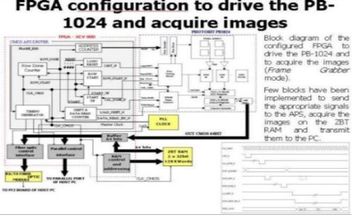
The electrons generated in a photocathode are multiplied by the MCP, and the emerging electron cloud impinges on a phosphor screen giving a luminous spot. A relay optics re-images this spot onto the CMOS-APS. The APS and a high density Field Programmable Gate Array (FPGA) are located on the same board that is connected to a PC through a parallel interface and a fast serial connection (1.2 GBit/s) based on fiber optic. The FPGA is configured to drive the APS, to readout the pixels and to make computations. The various functions are obtained by downloading the configuration file via the parallel interface by using a standard protocol or via the optical fibers by using a dedicated DLL. Finally the data corresponding to the coordinates of each valid event are acquired by the computer and stored in a file.
OPTICAL AND MECHANICAL LAYOUT
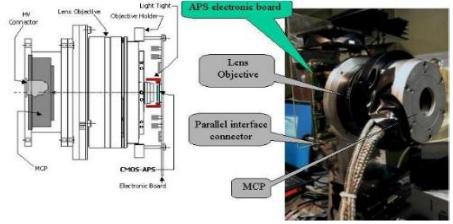 |
The CMOS-APS is usually delivered covered with a window, and, as for the CCDs, we planned to replace the window with a fiber optic taper. For the first tests we decided to use an optical objective, the Rodenstock model HR-Heligaron 35, with a very small numerical aperture (for better spatial resolution) and few optical components (to minimize the signal loss due to the transmittance of each element). The figure shows on the left side the mechanical layout and on the right side a picture of the complete system. |
THE CMOS-APS
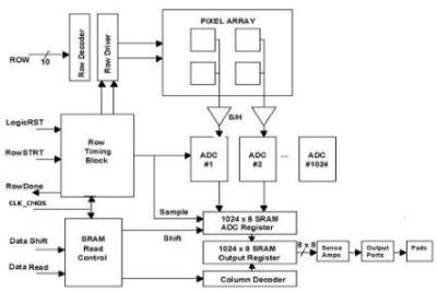 |
As position sensor of the photon counting system we used the CMOS-APS PB-1024 manufactured by Photobit that, with 500 frames/s, assures a high count rate and thus increases the system dynamic range. The internal architecture is shown in figure. The PB-1024 has been designed to have pixel row parallelism, in fact it includes on chip the timing and control circuitry to treat a row at a time (see the Row Timing Block on the schematic), and 1024 8 bit-A/D converters to digitize simultaneously the analog signal from an entire pixel row. Furthermore the chip contains special self-calibrating circuitry that allows to reduce the fixed pattern noise. To speed-up the data output a “ping pong” memory array is used. This type of memory stores the 1024 8-bit digitized data and is read during the next conversion cycle. Eight pixels (a 64 bit word wide) at a time can be read through the eight ports of 8 bits. Thus in 128 clock pulses an entire row is read-out. The device can be considered as a “digital device” in the sense that it receives digital signals and send digitized data. Thus, to drive the sensor only a “digital controller”, like a Field Programmable Logic Array (FPGA) is required. |
THE DRIVING ELECTRONICS
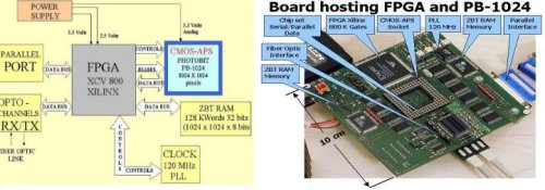 |
The block diagram of the detector front-end electronics is shown in the left panel of this figure, while a picture of the electronic board is in the right panel. The APS has on chip almost all the electronics needed to operate as an imager, the FPGA provides the rest of necessary signals. The implemented circuits on the FPGA provide the bias signals, their telemetry, that of the power supply, and the interface to the host PC. A 128 KWords 32 bits ZBT RAM is used to store the acquired image to be subsequently read at a different data rate. For example to drive the CMOS-APS as simple frame grabber a simple circuit has been implemented on the FPGA: |
 |
The heart of the controller is constituted by the implementation on the FPGA of the centroid algorithm, that essentially is divided into two parts: the event validation, that consists in locating the peak signal of all events above a specific discrimination level, and the centroid computation, that carries out a three point truncated center of gravity: if the pixel values are a, b, c, with b being the highest, the coordinate of the center will be (c-a)/(a+b+c). The following figure shows the block diagram of the implemented circuit. |
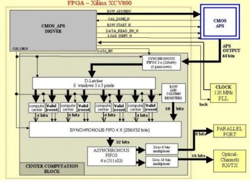 |
The 64 bits data, corresponding to 8 pixels, are stored on synchronous FIFOs at each pulse of the CLK_CMOS, and when the first three rows are completely packed on FIFOs, the computation procedure goes on. A set of D-Latches are used to obtain 8 windows of 3X3 pixels. The center computation and the event validation circuits operate simultaneously on these 8 windows, and, at each clock pulse, other eight 3x3 pixels windows are stored in the D-Latches, and the process continues until the end of frame. When the four synchronous FIFOs receive the validation event signal, they store the row and column data (contained in the respective registers) and the sub-pixel value (given by the center computation circuitry) to form a 32-bit word with the event x-y coordinates to be sent, through 4 asynchronous FIFOs and a multiplexer, to the host computer via the parallel interface or the fast serial link. |
| The incoming pixels are packed in two 8X3 pixels windows: “Current” and “Previous”. At each clock pulse 8 windows of 3X3 pixels are formed by swiping a 3X3 pixels box through the last two columns of the “Previous” window and the entire “Current” window. The centroid computation is carried out simultaneously on all boxes. The algorithm gives a resolution 1/32 of pixel. The figure shows the sheme of the centroiding processing. | 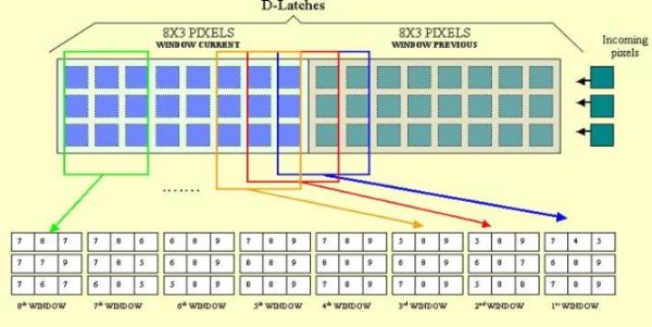 |
CONTROL SOFTWARE
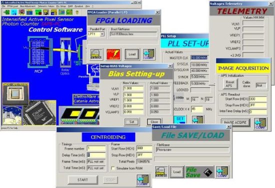 |
A control software has been developed to drive the entire acquisition procedure. It is written in Visual C++ and is organized as a series of dialog boxes. As can be seen from the following figure, the start-up window contains all the available commands that can be selected both from the main menu or from the icons menu. The “FPGA LOADING” allows to configure the FPGA, the “PLL SET-UP” allows to change the working frequency, the “BIAS Setting-up” permits to set the bias voltage levels of the APS, the “TELEMETRY” dialog box, when invoked, displays the current values of the biases, the two dialog boxes “IMAGE ACQUISITION” and “File SAVE/LOAD” allow to acquire an image and store it in a file. Finally the “CENTROIDING” allows to acquire directly the centroid event during the exposure time. |
FIRST RESULTS
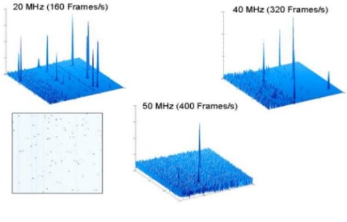 |
Before operating in centroid mode, we took lots of images, varying the MCP gain, the objective focus and the APS working frequency. From the analysis of the spot profile with respect to the noise level we derived the best operating conditions. An image of 512X512 pixels acquired at a frequency of 20 MHz is shown in the lower left panel of the figure And thus we can conclude that: the CMOS-APS used as position sensor in MCP based systems can perform better than a faster CCD and with some important advantages: compactness, simplicity, radiation hardness, low power consumption, low cost.
|