Catania Astrophysical Observatory Laboratory for Detectors
")
")
Detection of ultraviolet (UV) light from Sun, from astronomical objects or from artificial sources has received a great attention in the last years. A particular interest is focused on the numerous applications that require the visible light rejection such in the medical, military, environmental and astrophysical fields. Furthermore, the fabrication of high sensitive diodes array is very attractive for spectroscopic and UV imaging applications. In this context, wide band gap materials are excellent candidates for UV “visible blind” detection, being silicon carbide (SiC) the one having the highest maturity in terms of material quality suitable for electronic device fabrication. Among the polytypes of SiC, the 4H-SiC is preferable for “visible blind” detection, thanks to its wider band-gap (~ 3.3 eV).
Schottky photodiodes were fabricated on a 5.8 µm thick n-type 4H-SiC epitaxial layer, with a doping concentration of 2.7×1015 cm-3, grown by ETC S.r.l. on a hot wall horizontal reactor (ACiS M8 by LPE) onto a heavily doped substrate. Ohmic contacts on the sample rear were formed by e-gun evaporation of a 200 nm Ni film, followed by a rapid annealing at 950°C. Schottky contacts on the sample front side were obtained by defining self-aligned nickel silicide (Ni2Si) micrometric interdigit structures. The Ni2Si stripes (3 - 6 µm wide and spaced) were defined by standard lithography processes. The front electrode geometry allows the direct exposure to the radiation of the OAA and the vertical electrical operation of the Schottky diode. Rapid thermal annealing was used for the formation of Ni2Si and to improve the uniformity of the Schottky barrier with respect to that of pure Ni.
The single diode area directly exposed to radiation and electro-optically active was about 48 %, while the distance between contiguous pixels was about 25 µm. A not-in-scale diagram of the interdigit vertical Schottky structure and a top view microscope image of a part of an interdigit diode (bottom left corner of the Figure 1) are shown in the following figure.
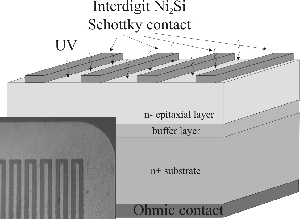
Figure 1. Not-in-scale diagram of the vertical Schottky UV detectors; in the left-bottom corner, top view microscope image of a part of the front electrode, showing the metal stripes.
A figure of merit of a photodiode is the quantum efficiency (QE), describing the probability that an incident photon generates an electron-hole pair. The values of the external QE were obtained comparing the photo-response of the tested detector with that of the reference one using the set-up described in characterization. To avoid under estimation of the QE, during the electro-optical characterization the irradiation beam (about 1 × 2 mm2 in size) was focused in the central region of the array, as verified by photocurrent measurements done activating single pixels of the array. The external QE of the total array was measured at 0 V (photovoltaic operation mode, straight line in figure) and -30 V (▲ in Figure 2) and it is reported in the next Figure.
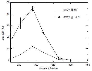
Figure 2. External QE versus wavelength of proposed array at 0 V and -30 V (▲).
We observe a relevant increase of the QE in the presence of reverse bias with respect to the photovoltaic condition clearly due to the increase of the OAA. The detector sensitivity reaches its maximum, between the investigated wavelengths, at 289 nm and is about 45 %.
The ultraviolet-visible rejection ratio, defined as the ratio between the sensitivity peak and the sensitivity in the visible (@ 405 nm), is > 4 ×10³ @ - 30 V.
Next Step: Silicon Carbide Photomultiplier (SicPM)