Catania Astrophysical Observatory Laboratory for Detectors
")
")
Here are presented some test measurements aimed to evaluate the performance of a Single Photon Avalanche Diodes (SPAD) developped by ST Microelectronics.
SPAD is a p-n junction biased above the breakdown. In this operative condition a hole-electron pair, generated in the depletion layer causes an avalanche, measurable as a current. The diode works as a single photon detector with an infinite gain. Figure 1 shows the structure of the last generation SPAD and that of the layout of an array. The current flows in the diode until the drive circuit, the active quenching circuit (AQC), turns off the polarisation for a dead time and then restores it. In this way the SPAD is ready for another event. This turn off time, defined ‘hold off’ time, depends basically on the quality of the SPAD. Figure 2 shows the block diagram of the quenching circuit that is made by a DRIVER that provides the polarization, a COMPARATOR that triggers the monostable when an event occurred. The monostable generates the hold-off pulse.
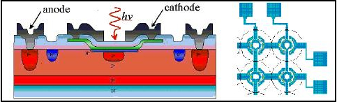
Figure 1. Structure of a SPAD device (left) and the array layout (right).
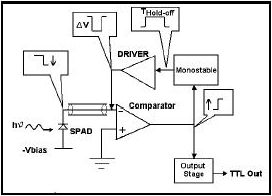
Figure 2. Active–Quenching Circuit Block Diagram
SPAD CHARACTERIZATION
The instrumental apparatus used for the quantum efficiency measurements is that described on the web page. The characterization system has been arranged to allow the optical interfacing with the SPAD head. Infact, after being dispersed the beam enters an integrating sphere, where the SPAD and a calibrated photodiode are mounted. The acquisition system reads, at the same time, the counts of the SPAD and the current measured by the calibrated photodiode. Prior to measure the QE of SPADs of different active areas (10, 20, 50 and 100 µm), we measured the breakdown voltage of each device and set the polarization voltage value between 10% and 20% above this value. A typical breakdown voltage is about 30 Volts. The SPAD quantum efficiency, measured in the range 350 - 1050 nm, is typical of a silicon based detector and shows a peak of about 60 % at 550 nm for 100 µm diameter devices. We measured the QE at different polarization voltages and found that the QE increases with the polarization voltage. The measurements show also an increase of the efficiency with the SPAD diameter. This result is unexpected because the QE measurements are normalized by area. One hypothesis is that there is a small area around the pixel with poorer sensitivity, due to fabrication process. In fact, the effect becomes less evident for devices with larger area.
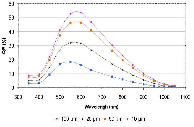
Figure 3. Quantum Efficiency at polarization voltage 20% above the breakdown voltage.
Dark counts
Dark current can be produced by thermal generation and after pulsing. Dark counts increases with the bias voltage because the higher electric field increases the probability of avalanche and the depletion volume. After pulsing depends on the following phenomenon: during the avalanche, some carrier can be trapped in the depletion layer and released after a time delay. If this time delay is greater than the hold-off time, the carrier generates an avalanche named “after pulsing”. To reduce the after pulsing effect, the hold-off time had to be increased although this reduces the count rate. Both causes of dark counts depend on the defects in the depletion volume and can be reduced with a cleaner fabrication process. Dark counts are measured at 20°C, with a hold-off time of 360 nsec that reduces the after pulsing effect. In Table 1 the results of dark measurements of 20 µm SPAD versus bias voltages are shown. The results highlight the dependence of dark counts by the bias voltage.
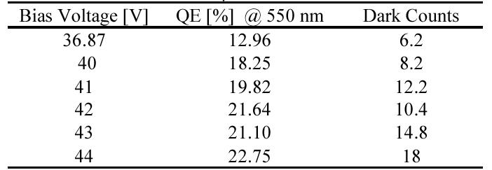
Table 1. Dark counts of a 20µm SPAD at 20°C.
Linearity
The linearity is measured using a standard method, consisting of illuminating the detectors at different signal levels with a uniform source of radiation. In Table 2 the deviation from linearity is shown. The measurements show that the deviation from linearity is very low and that there is not variation in QE in the range of measurements.
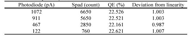
Table 2. Linearity of a 50µm SPAD.
Two arrays of 5 X 5 elements, with pixel size 20 and 40 µm of diameter, have been developed by STM and a series of test measurements have been carried out at our lab.