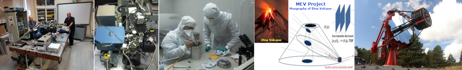
Catania Astrophysical Observatory Laboratory for Detectors
")
")
Optical Cross Talk evaluation through Dark Stairs measurements
The CITIROC 1A evaluation board part used to obtain staircase measurements is depicted in Figure 1. The SiPM pulse is amplified by the High Gain (HG) preamplifier and then is shaped (15ns shaping time) by the Bipolar Fast Shaper. A discriminator with a programmable threshold (10 bit DAC) is used to drive the output signal through the OR32, and in turn, sent to the counter inside the FPGA evaluation board
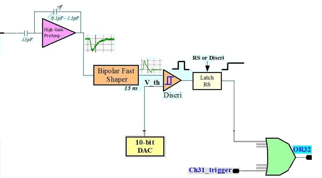
Figure 1. Block diagram of the used electronics inside the ASIC for staircase measurements.
The adopted method essentially consists in measuring the trigger rate as a function of the discriminator threshold in dark condition. Usually data are accumulated in 70 seconds. The result for a particular SiPM detector, the MPPC LVR2 3050CN, is shown in the Figure 2, where the characteristic staircase function is represented.
Assuming a Poisson distribution, the probability to have two coincident events within a time window of 15ns is about 10-2% (rate 100 Hz), negligible with respect to the dark rate measured.
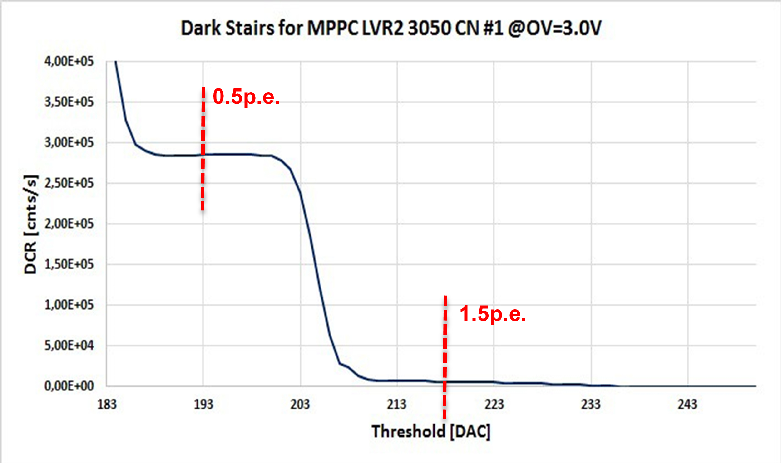
Figure 2. Dark Stairs measured for the MPPC LVR2 3050 CN at 3.0V of overvoltage.
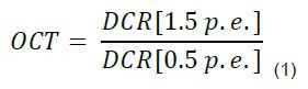
The Optical Cross Talk (OCT) level is evaluated from the ratio between values of DCR[0.5pe] and DCR[1.5pe] as indicated by the formula (1)
For the specific case of the MPPC LVR2 3050CN, being the DCR 5,78x10³ Cnts/s at 1.5p.e. and 2,85x10⁵ Cnts/s at 0.5p.e., by applying the formula (1) an OCT of ∼ 2% is obtained.
Influence of the front-end electronics on the measurements of DCR and OCT
Before discussing the OCT results, we have to introduce two problems:
In fact, using the formula (1), if the DCR at 0.5 p.e. is underestimated and the DCR at 1.5 p.e. is overestimated we obtain an OCT overestimated.
Thus, we will have two effects that can give false OCT values:
In both cases, the OCT will result higher than that effective.
Independently from the above-mentioned effects, the OCT rises with the sensitive area because the probability to have the LED emission effect is directly proportional to the number of microcells. Another important parameter that play an important role in OCT performance is the presence of the protective coating on top of the sensitive surface. In other words if the pile-up and the inefficient ZPC effects are neglected, the OCT will be higher for SiPMs with higher dimensions and with s ilicone coating.
While the second effect is impossible to remove or adjust because the derivative circuit is inside the ASIC chip, the first effect can be mitigated because depends on the count rate. Lowering the temperature the DCR will fall down and thus the pile-up probability will decrease. We have investigated the pile-up effect on the bare devices LVR2 3050 CN, LVR2 6050 CN and LVR2 7050 CN by measuring the OCT at 3V of OV as function of the temperature or, in turn, as function of the DCR. The result is shown in Figure 3.
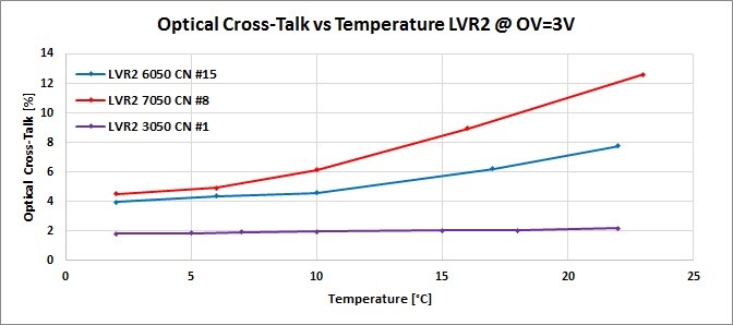
Figure 3. OCT versus temperature for the bare devices LVR2 3050 CN, LVR2 6050 CN and LVR2 7050 CN.
As can be noted for temperatures below 6°C, the LVR2 6050 CN shows an OCT around 4%, the LVR2 7050 CN shows an OCT around 5%, while the LVR2 3050 CN, being a device of small size, shows an OCT of 2% at any temperature. It seems also that below 6°C the pile-up effect does not influence the OCT measurement for the large detectors and the difference (about 1%) is only due to the different dimensions.
We have characterized SiPM Hamamatsu detectors LCT5, LVR and LVR2 series. The detectors are listed in Table 1
|
Device name |
Dimensions [mm2] |
Pich size [µm] |
Coating |
BV @25°C [V] |
Gain @3V OV |
DCR @6°C [cnts/s] |
|
LCT5 3050CS |
3 x 3 |
50 |
Silicone |
52.50 |
2.0x10⁶ |
|
|
LCT5 7050CS |
7 x 7 |
50 |
Silicone |
52.80 |
2.0x10⁶ |
3.41 x10⁵ |
|
LCT5 3075CS |
3 x 3 |
75 |
Silicone |
51.30 |
3.3x10⁶ |
|
|
LCT5 6075CS |
6 x 6 |
75 |
Silicone |
52.01 |
3.3x10⁶ |
2.54 x10⁵ |
|
LCT5 7075CS |
7 x 7 |
75 |
Silicone |
52.70 |
3.3x10⁶ |
4.00 x10⁵ |
|
LVR 3050CS |
3 x 3 |
50 |
Silicone |
36.80 |
2.8x10⁶ |
|
|
LVR2 3050CN |
3 x 3 |
50 |
Bare |
38.26 |
2.8x10⁶ |
|
|
LVR2 7050CS |
7 x 7 |
50 |
Silicone |
38.20 |
2.8x10⁶ |
7.96 x10⁵ |
|
LVR2 7050CN |
7 x 7 |
50 |
Bare |
38.60 |
2.8x10⁶ |
6.52 x10⁵ |
Tabella 1. Elenco dei rivelatori SiPM caratterizzati
We measured the Optical Cross Talk (OCT) respect to overvoltage (OV) from 2V to 6V in 1V steps.
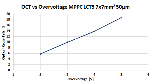
The obtained results are subdivided by technology (LCT5 or LVR). Figure 4 shows the OCT plots of the 3x3mm2 LCT5 devices with 50 μm microcells (left) and 75 μm microcells (right). Figure 5 shows the OCT plot of the 6x6mm2 LCT5 MPPC with 75 μm microcells. Figure 6 shows the OCT plots of the 7x7mm2 LCT5 devices with 50 μm microcells (left) and 75 μm microcells (right).
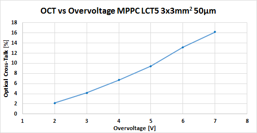 |
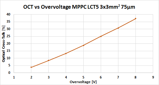 |
Figure 4. Optical Cross-Talk versus Overvoltage for 3x3 mm2 LCT5 devices with 50μm microcells (left) and 75μm microcells (right).
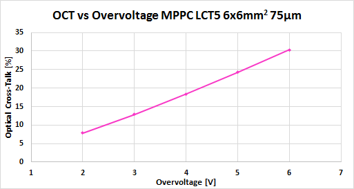
Figure 5. Optical Cross-Talk versus Overvoltage for the 6x6mm2 LCT5 SiPM with 75 μm microcells
 |
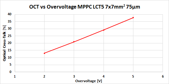 |
Figure 6. Optical Cross-Talk versus Overvoltage for SiPM LCT5 7x7 mm2 LCT5 devices with 50μm microcells (left) and 75μm microcells (right).
We compared all the LCT5 devices in Figure 7.
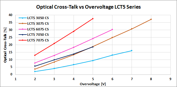
Figure 7. Optical Cross-Talk versus Overvoltage for all the SiPMs LCT5 series.
As expected, the OCT rises with the SiPM dimension.